November 25, 2025
April 21, 2008
Introducing 74HC193 Simulation to LTspice
[tag]Ron Fredericks[/tag] writes: I have completed the design and test of a new [tag]component[/tag] for [tag]LTspice[/tag]/[tag]SwitchCAD III[/tag] [tag]circuit simulation[/tag] and [tag]schematic capture[/tag]. In a previous post I discussed my interest in the [tag]74193[/tag] presettable synchronous 4-bit binary up/down counter [tag]IC[/tag] for a digital volume control circuit I am building. The [tag]circuit[/tag] [tag]simulation[/tag] described below focuses on how to simulate the 74HC193 IC, but [tag]timing[/tag] and [tag]voltage[/tag] parameters built into this design allow a designer to easily simulate other variants of this IC from high speed Si-gate [tag]CMOS[/tag] HC and HCT devices to low power [tag]Schottky[/tag] [tag]TTL[/tag] devices.
All circuits related to this 74HC193 simulation are available here>
The 74HC193 Component
See figure 1 below for a screen shot of the completed design. The circuit was built from the digital gates in the component library supplied with the original [tag]Linear Technology[/tag]’s free LTspice tool.

Figure 1 – 74HC193 Circuit and Related Components
View larger image>
To keep the design looking like the original data sheet logic diagram, as published by companies that include NXP Semiconductors and Texas Instruments, a custom “T notS-R FlipFlop” subcomponent and corresponding assembly file was first created. This subcomponent was reused 4 times in the main IC logic diagram. An assembly file called 74hc193.asy was also created. It includes all pins used on the commercial IC except ground and Vcc. The IC’s internal power supply is not simulated by the Linear Technologies’ gates, and so they are not used or required in this design either.
Each gate within the design has a few variables assigned to them so that the IC remains flexible and easy to reuse in new projects:
- tdgate
 td (propagation time delay assigned to each gate)
 - tdgate2 td (propagation time delay assigned to the D FlipFlop)
- tripdtgate tripdt (td’s accuracy band assigned to each gate including the D FlipFlop)
- vhighgate logical high value for each gate and D FlipFlop
- vlowgate logical low value for each gate and D FlipFlop
These variables can be assigned their corresponding time and voltage values using a .param statement placed in the main circuit. These values are then within scope for automatic reuse by the 74HC193 component and flipflop subcomponent simulations. Below is an example of how parameter assignment can be made (as used in the test circuit described next):
.param tdgate=10n tdgate2=3*tdgate tripdtgate=1n vhighgate=5v vlowgate=0v
April 15, 2008
New Gate Design Using LTspice/SwitcherCAD III
[tag]Ron Fredericks[/tag] writes: recently I discovered that I was going to have to create my own IC [tag]component[/tag] and symbol for my on-going digital volume control [tag]circuit[/tag] [tag]simulation[/tag]. My first step was to check in with the [tag]LTspice[/tag] forum on yahoo groups. On the forum I requested any previous design for the IC I needed. I also asked the group’s readership if they thought it was correct to build a new IC from existing low level digital gates – gates that are already supplied with the LTspice distribution by [tag]Linear Technologies[/tag].
Well, I did not find a previous inventor for my IC simulation, but I did get confirmation that the gate build-up was a common strategy. And, this same forum engineer supplied me with a copy of an IC simulation of his own – one very similar to my IC requirement – he supplied a symbol and sample test bed to accelerate my learning curve. Here is a link to my support dialog.
I would like to thank [tag]Helmut Sennewald[/tag] for his time and excellent service to the LTspice yahoo forum. It is his effort and many others who make this forum such a valuable community resource. This forum in turn, has made the LTspice/SwitcherCAD III circuit capture and spice tool a viable design tool for many [tag]embedded[/tag] component users and EE designers.
Introducing the T S-R Flip-Flop
To build my new IC, I had to build a new digital logic block. This component is a Toggle Flip-Flop with Set and Reset functions added. In this blog post I introduce my readers to this new component and share the simulation circuit for others to use and learn from.
See the figure below for an initial design of the T S-R Flip-Flop, including a truth table in the form of a waveform diagram, the circuit, a pulse detector sub-circuit and their related assemblies. This circuit is just an initial design because it uses an S-R Flip-Flop and a simple pulse detector sub-circuit for its clock.

View larger image>
Final Design for the T S-R Flip-Flop
This section of my post is an update, thanks to a review by Helmut Sennewald. See figure below for my final design of the Toggle S-R Flip-Flop. This design overcomes two problems in my initial design, both resolved by starting with the D Flip-Flop with its built-in clock. The reuse of this more full-featured LT supplied component in my design eliminated the home-brew pulse maker sub-circuit. And in so doing, the slower S-R Flip-Flop. Slower because I had to set the SpiceLine time delay to a minimum of 20 nanoseconds (or td >= 2x the gate time delay) to support the simulation of my simple pulse maker sub-circuit. The D Flip-Flop has an internal clock so I could eliminate the pulse maker sub-circuit. End result: one less sub-circuit and faster Flip-Flop simulation using a time delay set to a minimum of 10 nanoseconds (or td >= 1x the gate time delay).

View larger image>
Download
To test my knowledge of digital design using the LTspice tool, I created a number of similar flip-flop components which are included in the download:
- S-R Flip-Flop test circuit
- S-R Flip-Flop with Enable gate and test circuit
- S-R Flip-Flop with rising edge clock and test circuit
- J-K Flip-Flop with rising edge clock and test circuit
- D Flip-Flop with Enable gate and test circuit
- T S-R Flip-Flop from S-R Flip-Flop and test circuit (initial design)
- Rising Edge Pulse Detector (not high performance design)
- T S-R Flip-Flop from D Flip-Flop and test circuit (final design)
Download the components listed above for your LTspice designs all in one zipped directory.
March 26, 2008
Simulating the 555 IC with LTspice
[tag]Ron Fredericks[/tag] writes: I was designing a simple CMOS timer circuit around a 555 chip this evening. It might be the heart beat for a new digital volume control I have been thinking about. Normally I look for my breadboard and parts box but this time I thought I would try out Linear Technologies LTspice/SwitcherCAD III workbench instead.
SwCAD III First Time Use
The tool is free and comes with a lot of support. I downloaded the software and installed it very easily on my Windows XP PC. It includes a graphical [tag]schematic[/tag] design tool with lots of ready made simulated components, including an NE555 for my initial project. Designing the circuit with the built-in CAD tool works very intuitively. While the LTspice simulation took a bit of head scratching before it worked for me.
I was able to configure and run the simulation using the drop down tools menu and the little “running person” icon on the tool bar. But all I could get out of the simulation was a black screen with voltage and timing ticks along the left and bottom edges. So my first problem was in realizing that the visual display would remain black and traceless until I put the mouse cursor over a wire then click. When the little instrument probe showed up as my mouse icon, I realized what was going on here. With the mouse click, waveform tracings would appear in the black panel.
My second problem was that the circuit would not oscillate. Not good for an oscillator design. First, I forgot to connect the 555’s threshold + trigger pins to the R2-C2 node using the wire tool. But still no oscillation, just flat line traces were observed. Now I already know that getting circuits to oscillate follows Murphy’s Laws: Oscillators remain stable, Amplifies and Buffers oscillate, whenever possible. I found a note on the Old School Hacker blog with a fine solution. You must simulate the circuit with a power supply starting from 0 volts rather than just have an instant on Vcc power supply.
In hind sight dah, its the initial transient response from the circuit’s components that kicks the oscillator into oscillating.
After a little practice I improved the schematic diagram with the use of named nodes and seperation of the temporary load resistors R3 and R load from the more permanent circuit components. The load resistors are just place holders for a real load to be added to the circuit schematic next. Look for my next blog post on this subject.
Finally, I used the cursor measurement facility built into the LTspice window (trace window). With this feature, I was able to make “real” measurements on the waveform for frequency and duty cycle.
Circuit
Here is what I was able to generate using the [tag]LTspice[/tag]/[tag]SwitcherCAD III[/tag] tool:
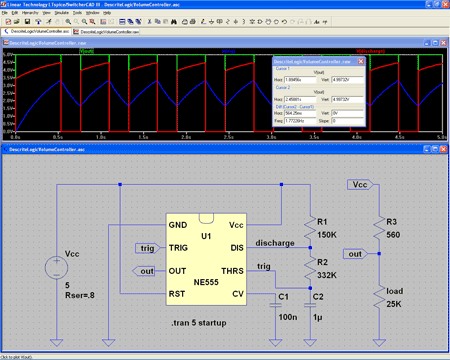
View larger image>
Download 555 Astable Flip-Flop Schematic Circuit Diagram>
Referring to the figure above:
Green Trace -> Output (IC 555 pin 3)
Blue Trace -> Trigger / Threshold (IC 555 pins 2 & 6)
Red Trace -> Discharge (IC 555 pin 7)
The Astable Multivibrator
The circuit shown above will trigger itself and free run as a multivibrator. The capacitor C2 charges through resistors R1 and R2 yet discharges through R2 only. Thus, the duty cycle (D) may be precisely set by the ratio of these two resistors. The capacitor charges and discharges between 1/3 Vcc and 2/3 Vcc. But the initial pulse charges C2 starting from 0 Vcc and so this first pulse duty cycle is unique. Since the charge rate and the threshold levels are directly proportional to the supply voltage Vcc, the frequency of oscillation (f) is independent of the supply voltage.
| Frequency Calculation | Duty Cycle Calculation |
|---|---|
C_2}") |
 |
 ohm farads}") |
 |
| Measured = 1.8 hertz | Measured = 0.60 |
Where: is frequency in hertz is frequency in hertz is capacitance in farads is capacitance in farads is resistance in ohms is resistance in ohms |
Where: is duty cycle is duty cycle is non-zero output duration is non-zero output duration is the period of the output is resistance is the period of the output is resistance |
Reference
- 555 Datasheet icm7555.pdf
- Linear Technology’s SwitcherCAD™ III Landing Page
[tags]simulator, Spice, CAD[/tags]